[This is a sponsored article with Selangor Information Technology & Digital Economy Corporation (Sidec).]
For decades, Malaysia has played a crucial role in the global semiconductor industry, especially in assembly, test, and packaging (ATP). But higher-value activities like chip design, prototyping, and validation often happen elsewhere.
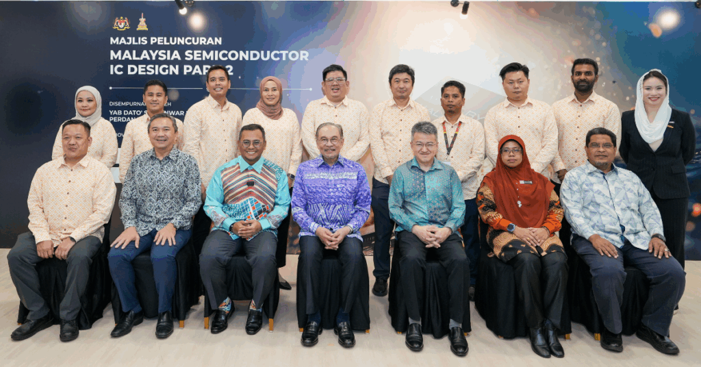
In a step to further our ambition, the government recently launched the Semiconductor IC Design Park 2 (IC Design Park 2) in Cyberjaya.
It was officiated by Prime Minister Dato’ Seri Anwar Ibrahim and Selangor Menteri Besar Dato’ Seri Amirudin Shari, marking the debut of Southeast Asia’s first Advanced Chip Testing Centre.
The facility serves as a hub for Malaysian engineers to fully design, emulate, test, validate, and commercialise semiconductor chips without needing to send prototypes overseas. For a nation historically dependent on foreign testing labs, this is a huge milestone.
Here’s everything we know about Southeast Asia’s first advanced chip testing centre.

Establishing a complete semiconductor ecosystem
Before IC Design Park 2, there was IC Design Park 1 in Puchong that launched back in August 2024 (which we also covered here). So you may be wondering, “Why open up a new facility so soon and so far away from each other?”
IC Design Park 1 in Puchong was established to focus on building the integrated circuit (IC) design core and incubate local semiconductor startups and design houses.
Over 400 engineers from 14 partnering companies (such as SkyeChip, Infinecs, Oppstar, Weeroc, MaiStorage, ICESB, Cortical Labs, WyseTime, and Alphaswift Industries) are given access to world-class EDA tools, IP libraries, and collaborative design labs.
The idea was to set up Malaysia’s design-led semiconductor base and talent pipeline.
But Puchong was only ever meant to set the foundation, not to house heavy lab operations. This is where IC Design Park 2 in Cyberjaya completes the ecosystem.

The addition focuses on testing next-generation chips used in a wide range of industries. This includes AIchips used in data centre servers and smart devices, automotive electronics particularly for EVs, Internet of Things (IoT) sensors and controllers, high-speed communication chips, and consumer and industrial electronics.
It houses four state-of-the-art labs needed to further expand our semiconductor industry to advanced testing and research:
- Advanced Chip Inspection, Test & Metrology Centre (AIM) (Pusat Pemeriksaan, Ujian & Metrologi Cip Termaju) – for wafer and substrate inspection, quality mapping, and metrology.
- Advanced Chip Design, Emulation & Prototype Centre (Pusat Reka Bentuk, Emulasi & Prototaip Cip Termaju) – for chip prototyping and system-on-chip (SoC) emulation.
- Advanced Chip Validation & Robotics Centre (Pusat Pengesahan Cip Termaju & Robotik) – for automation, functional testing, and robotics-assisted validation.
- Advanced Chip Research & Training Centre (Pusat Penyelidikan & Latihan Cip Termaju) – for collaborative R&D, workforce development, and upskilling under ASEM programmes.
Cyberjaya was the location of choice because the area offers the right ecosystem, infrastructure, and strategic location to support this next phase of Malaysia’s semiconductor ambition.
As a flagship city under the Malaysia Digital Initiative, Cyberjaya houses a dense concentration of data centres, global tech companies, innovation-driven institutes, and universities.
This environment provides the ideal ecosystem for collaboration, with advanced connectivity, digital infrastructure, and close proximity to federal agencies and industry partners.

Southeast Asia’s first world-class chip testing centre
One of the biggest announcements at the launch was the advanced chip testing centre, the first of its kind in the region. For years, local designers have had to send prototypes overseas for test and validation, which adds weeks of delay and significant costs.
Mr. Yong Kai Ping, Sidec’s CEO, explained why few countries have built facilities of this scale. “It’s not just about buying the machines. You need the right ecosystem, the right talent, and long-term policy support to make it sustainable.”
The investment needed for advanced inspection, automated metrology, and robotics-based validation is substantial, and many countries prioritised ATP because it’s faster and cheaper to scale.
It takes years of training for talents to master a mix of precision engineering, data analytics, and factory automation skills. The lack of a central ecosystem also means that even when prototypes are ready, commercialising them becomes a struggle because there’s limited access to anchor customers, pilot environments, and certifications.
Hence, Sidec and the Selangor state government decided to connect all these pieces into one place at IC Design Park 2.

“Crucially, we also provide direct go-to-market (GTM) support with industry partners: coordinated pilot projects, qualification pathways, access to enterprise customers in data centres, automotive, and aerospace, and partner-led programmes with leading tool and instrumentation companies.”
Mr. Yong Kai Ping, CEO of Sidec
What sets this new testing centre apart is its speed and precision. The facility features high-automation systems capable of inspecting and sorting up to 25 wafers in two minutes, which is much faster than most facilities, as well as spot even the smallest defects.
The talent engine powering this shift
Another major part of IC Design Park 2 is the expansion of the Advanced Semiconductor Malaysia Academy (ASEM), which aims to train 20,000 semiconductor engineers over the next decade.
The academy’s training is deeply industry-driven, delivered through partnerships with Arm, IIT Madras, Synopsys, Cadence, and Keysight.

The launch also celebrated the graduation of ASEM’s seventh cohort. Hundreds of students completed intensive six to eight month programmes combining classroom instruction, hands-on lab sessions, EDA workflows, chip design, validation, robotics, and embedded systems.
Thanks to Khazanah’s K-Youth Programme, many of them already have structured internship and job placement pathways with leading companies, such as AMD, Intel, Infineon, NXP, ASE, STMicroelectronics, and local ecosystem players.
IIT Madras Global is also working closely with ASEM on R&D and advanced training, including a specialised RISC-V architecture programme that sends Malaysian participants for a hybrid training experience in Malaysia and India.
Dictionary time: RISC-V architecture is an emerging global standard in open-source semiconductor innovation that is driving advancements in AI, automotive, and data centre applications.
Building Malaysia’s next-generation chip ecosystem

With Sidec driving the initiative and Cyberjaya providing the ecosystem, Malaysia seems equipped with the infrastructure, partnerships, and talent pipeline needed to compete in high-value semiconductor design and innovation.
IC Design Park 2 brings together state-of-the-art labs, industry-led training programs, and access to local and global partners under one roof.
This strategic combination of government support, advanced facilities, and skilled talent enables Malaysia to play a stronger and more integrated role in the global semiconductor industry.
For engineers, startups, and companies looking to be part of this journey, IC Design Park 2 offers a platform to innovate, collaborate, and shape the future of semiconductors in the region. More information can be found here.
- Learn more about the Semiconductor IC Design Park 2 here.
- Learn more about Sidec here.
- Read articles we’ve written about Malaysian startups here.
Featured Image Credit: Sidec